3D Chip Packaging
Up to 7x FLOPS/kWh
Memory and compute,
closer together
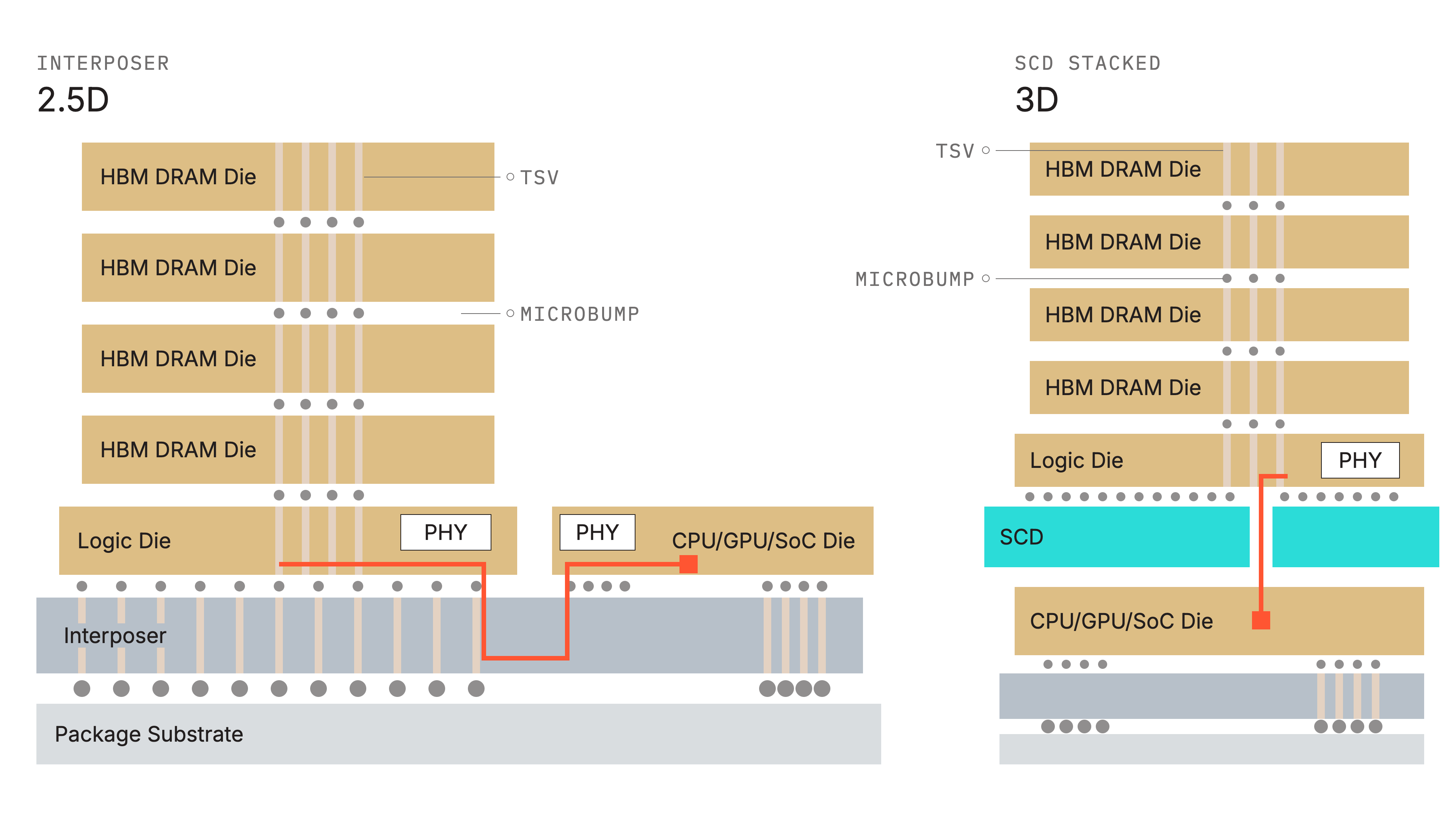
In CoWoS/EMIB 2.5D chip packaging worlds, compute dies and memory stacks are placed side by side on top of an interposer that provides the connectivity between them. This means the wiring is generally longer than the chip size of close to 33x26mm.
3D packaging reduces wire length by effectively 10x. This improves the energy needed to move data with I/O energy per bit improvements as high as 10x. It also reduces interconnect delays and capacitance by placing memory on top of the logic.
Cooling the 3D stack
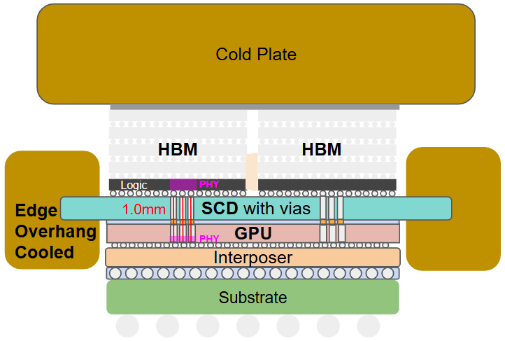
But this comes at the detriment of memory, which is heat-sensitive and now being effectively fried in the logic frying pan.
It turns out SCD interposers can help -- in a surprising way: Placed between memory and compute, SCD is so thermally conductive that it can pull heat out laterally over the entire chip size -- just by cooling it in a standard way at its edges.
This can enable 6.7x higher energy efficiency.
Read details in DF Tech Note 2512.