ALL-DIAMOND MOSFETs
Diamond Transistor
50x faster switching
In partnership with Stanford University, we are developing transistors that use diamond as a semiconductor.
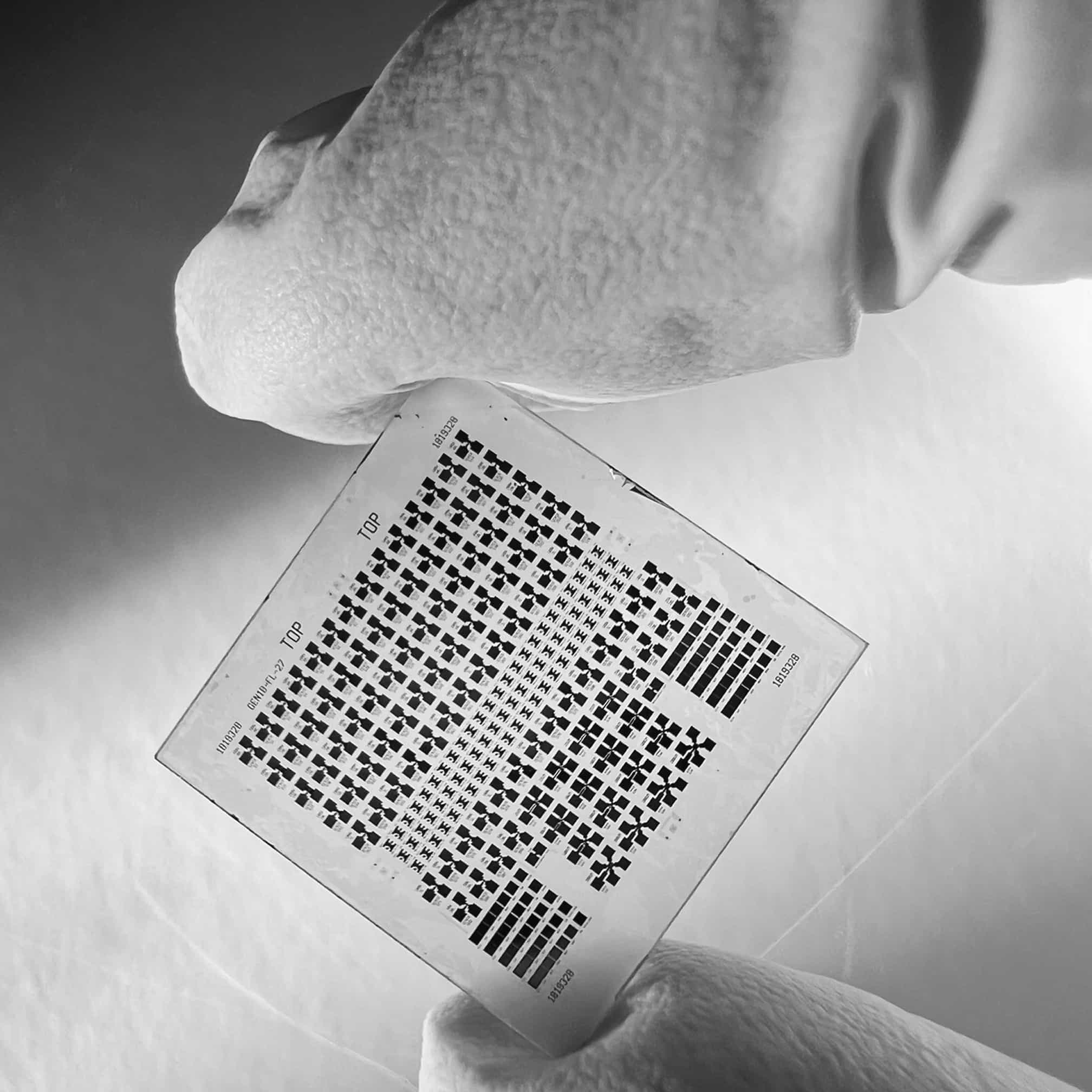
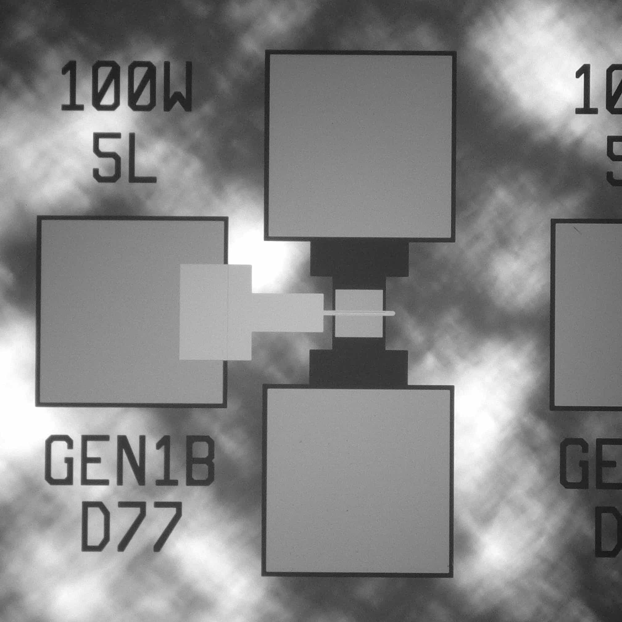
Surface transfer doping
Our all-diamond transistors use surface transfer doping to induce charge carriers without introducing substitutional dopant atoms into the bulk crystal.
DF Paper in IEEE: On the Conduction Mechanism in Diamond 2-Dimensional Hole Gas Field Effect Transistors
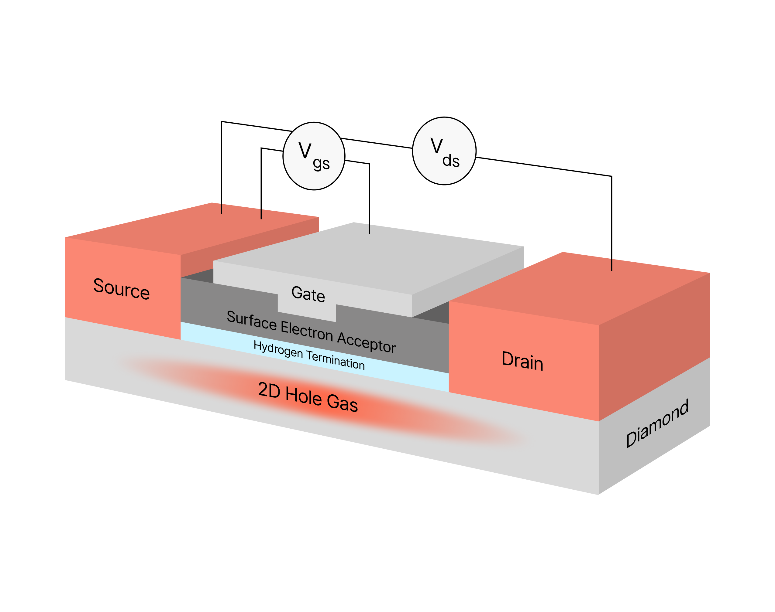
When the surface of a single-crystal diamond wafer is terminated with an atomic layer of hydrogen, its electron affinity becomes negative, allowing electrons to transfer from the diamond valence band to suitable acceptor species (often adsorbates or engineered surface layers) at the surface.
This charge transfer leaves behind a high-density two-dimensional hole gas (2DHG) confined within a few nanometers of the surface, producing p-type conductivity while preserving the intrinsic purity, thermal conductivity, and breakdown strength of the diamond bulk.
Because no ion implantation or lattice substitution is required, surface transfer doping avoids defect generation and carrier scattering associated with conventional doping, making it particularly attractive for high-power, high-frequency, and radiation-hard electronic device platforms.
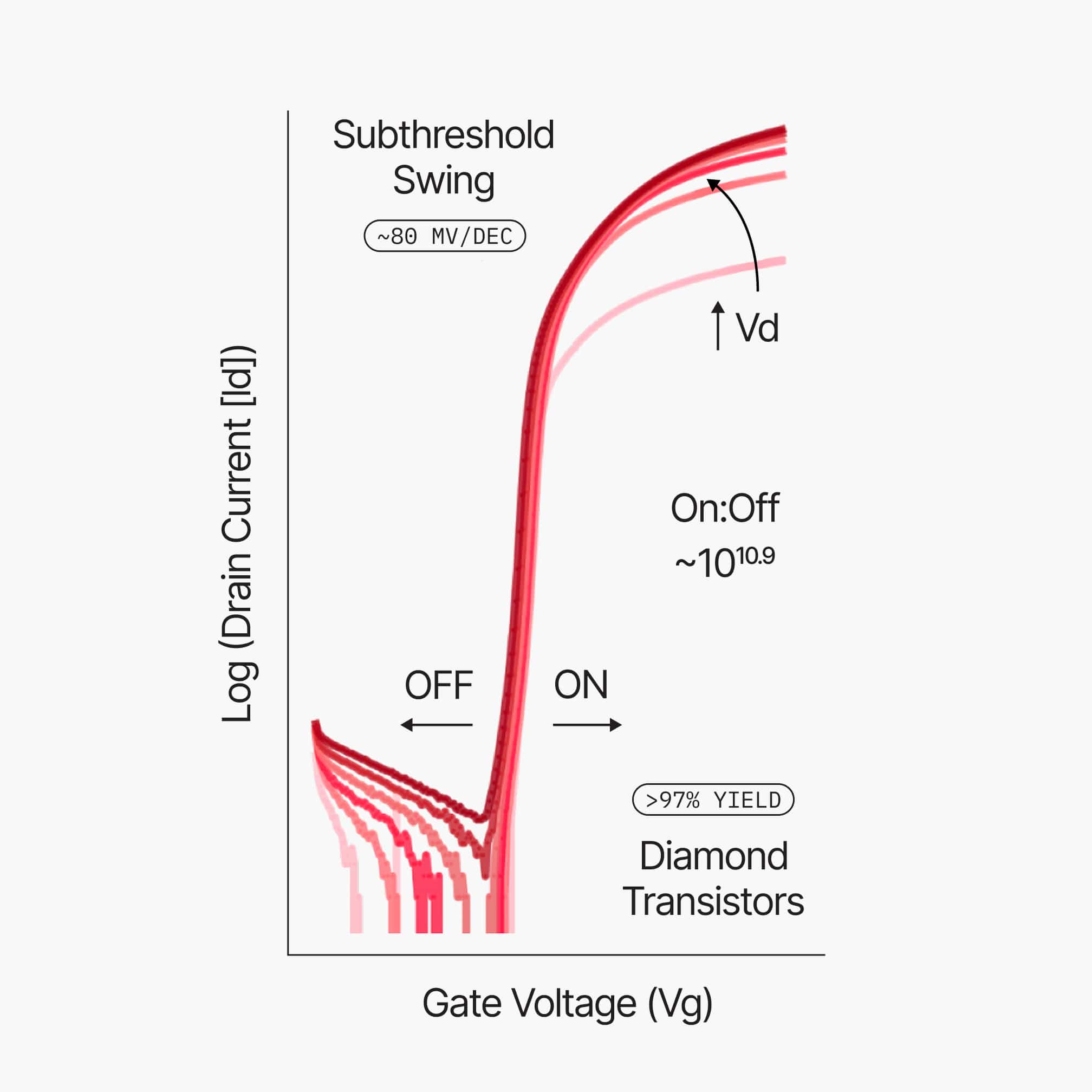
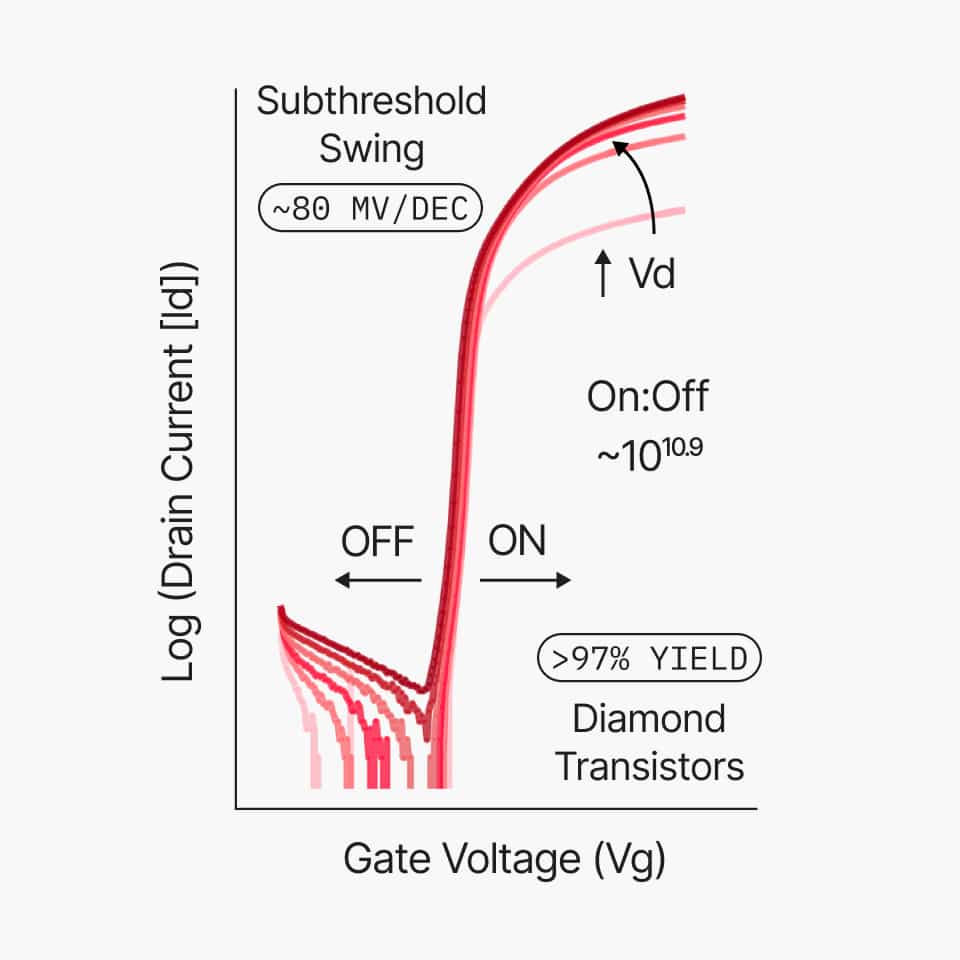
Matching silicon in subthreshold swing
DF devices now match state-of-the-art 3 nm silicon in subthreshold swing.
R&D Partnerships
Building your own diamond transistors?
We supply diamond substrates to R&D groups developing diamond transistors.
Learn more about the innovations that have made this possible.
DF Insights
Our latest news and industry know-how.
Nov 25, 2025
DF adds $2.77B fab in Spain
Nov 4, 2023
WSJ: Diamond Key to Faster Microchips
Oct 2, 2023