World’s first diamond wafer
A milestone in the history of technology

Once every few decades:
A new single-crystal wafer


Direct IC wafer bondable
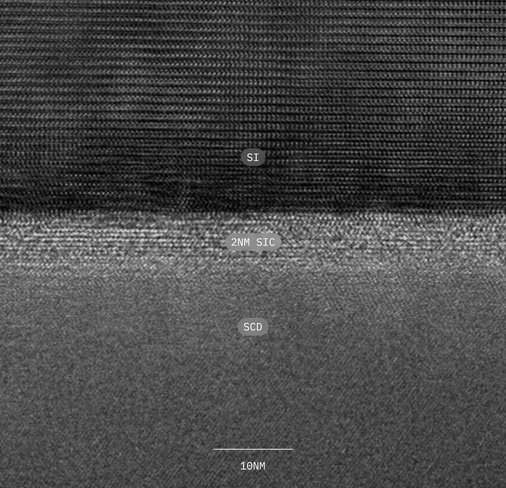
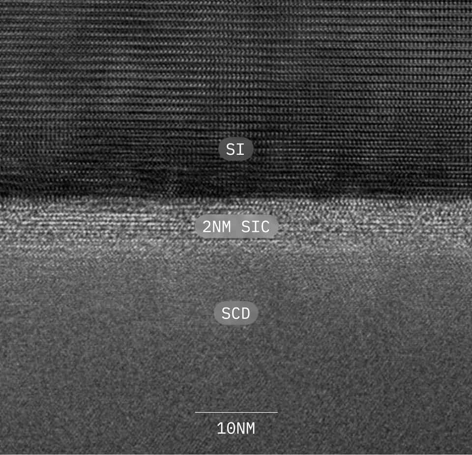
We achieve the ultimate thermal chip package by bonding our diamond atomically to integrated circuit (IC) wafers thinned at Angstrom precision.

Ultimate thermal conductor
No other material conducts heat as efficiently as single-crystal diamond, enabling chips to run faster and last longer.

Extreme electrical insulator
The thinnest slice of diamond insulates against very high voltages, enabling the next level of miniaturization in power electronics.
Mega techs, accelerated
We accelerate today’s most exciting mega-tech industries — each limited thermally at their technological core — by putting a diamond behind every chip.
A scientific and technological milestone
The pinnacle of decades of scientific research and development, our diamond wafer is a structure previously non-existent in the universe as well as the largest diamond on Earth.

DF Insights
Our latest news and industry know-how.


