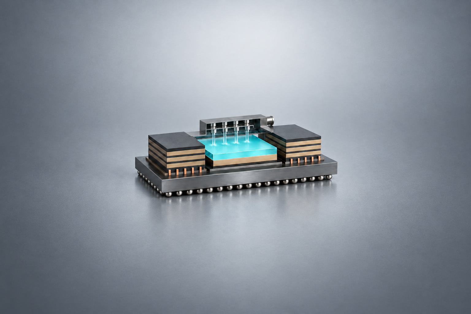
SCD Substrating
Hotspot-Free AI Chips
Up to 10x Power
Up to 10x Lifetime
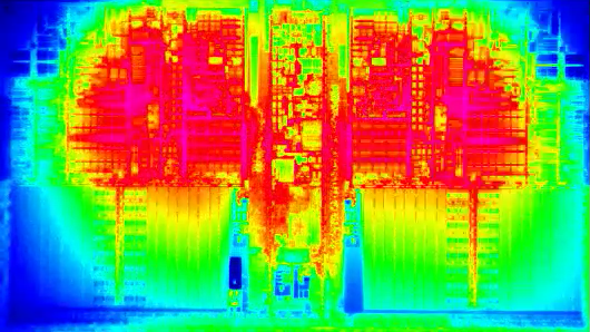
Hotspots are Evil. And Everywhere.
Hotspots limit chip speed and lifetime. Local peak temperatures are the key driver to constrain performance and accelerate chip failure mechanisms.
Hotspots occur in high-power training chips as well as lower-power inference chips. Even a chip that is cooler on average can contain microscopic regions with intense local heat flux.
Learn more about how hotspots are everywhere and how Hotspots are Evil.
Standard Silicon – but Thinned, then Substrated with SCD
State of the Art
Active Silicon 0.05 µm
Passive silicon
799.95 µm
TIM

Cold plate
Heat stays concentrated
SCD Substrated
Thinned Silicon 5–30 µm
SCD
600 µm

Direct cooling
Heat spreads laterally
Conceptual cross-section
Only the top 1% of silicon in a chip die is active transistors, etc. The remainder 99% is passive material, trapping heat because silicon is a poor thermal conductor.
Bonding SCD substrates within microns of the active silicon dissipates hotspots laterally, flattening temperature peaks as well as boosting downstream cooling to work more efficiently.
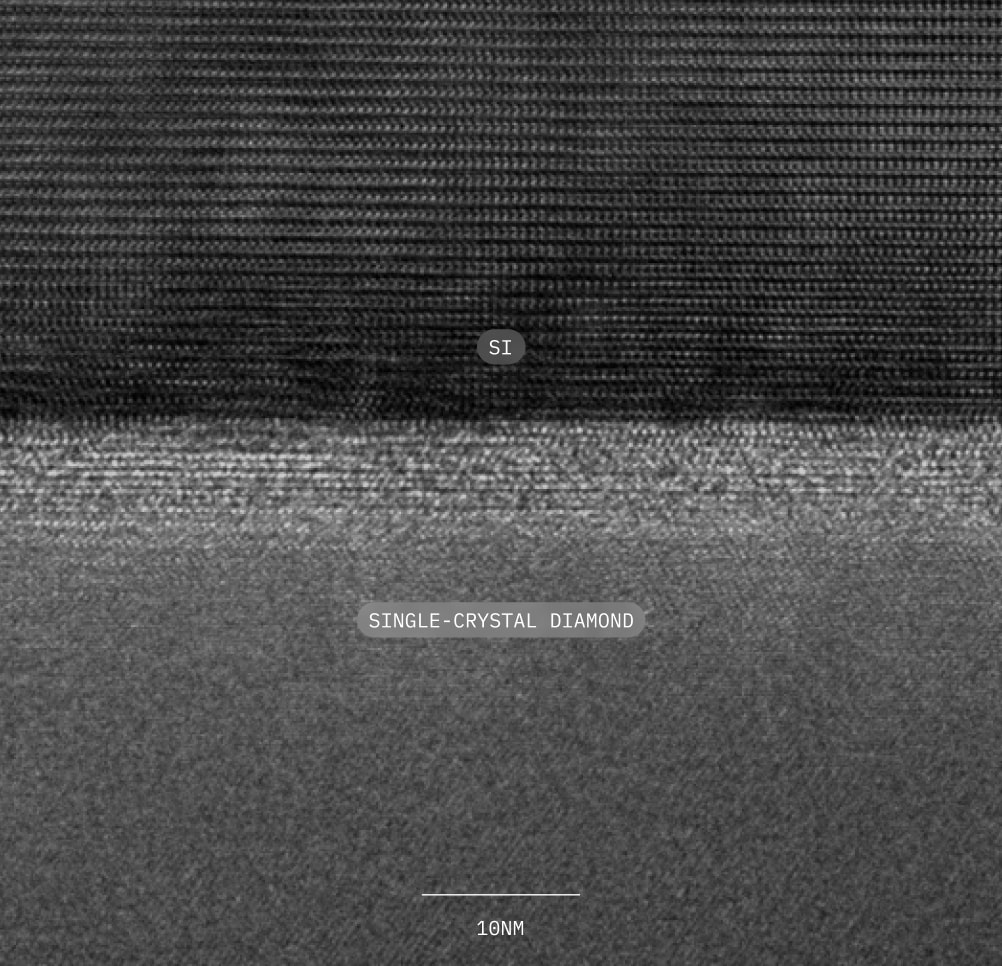
Silicon bonded directly to SCD.
Enlarge image →
Hotspots, Gone
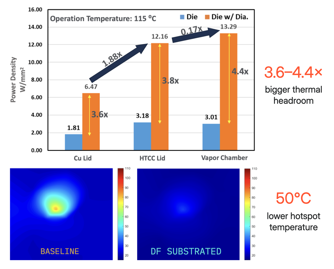
SCD substrating flattens hotspots – and enhances a chip’s thermal envelope to benefit speed and lifetime.
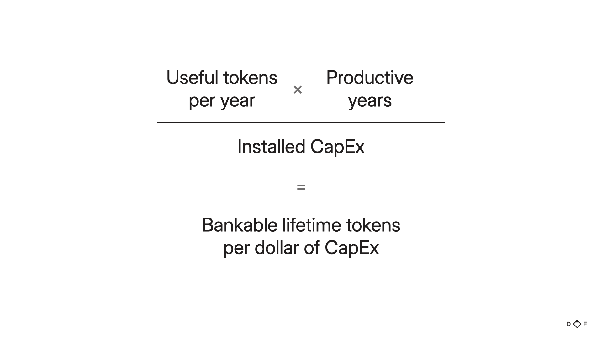
Chip designers can use the larger thermal envelope to increase performance, extend lifetime, or pursue a combination of both. Either choice can increase lifetime tokens per dollar of capital invested.
Bring SCD to your AI chips →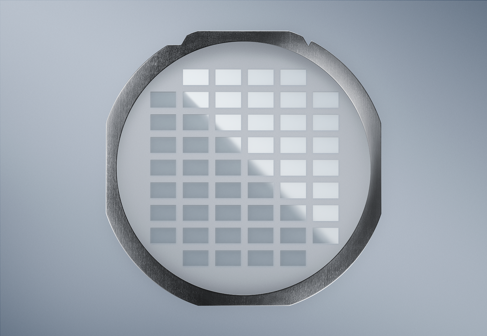
Chip Sized SCD Substrates: Now Exist and Available at Scale
Single Crystal Diamond substrates now exist at ASML reticle-limit size and are available in volume. (Just a few years ago, no-one on Earth knew how to possibly make them.)
Learn more about DF Operations →150
Silicon
380
SiC
400
Copper
3,000
SCD
Thermal conductivity (W/mK)
No Compromise
SCD is the no-compromise solution to thermal. Yes, there are other compromising ways to thermal:
Graphene or polycrystalline diamond?
SiC? An incremental benefit but not enough of a thermal envelope to make AI chips bankable.
Microchannels? Technically intriguing but plagued by operational and financial risk.
Make AI Chips Bankable
For AI chips to be a bankable infrastructure asset, they need to be engineered for it.
We help make AI chips bankable through one of the most controllable drivers for limited speed and lifetime: peak temperatures.
By giving AI chips their max thermal envelope, we enable chip designers to achieve max lifetime tokens through either faster speed or longer lifetime or any combination thereof.
Learn more about Making AI Chips Bankable →Explore the technology
We are working with the leading AI chip & cloud compute companies to create the future.
DF Insights
Our latest news and industry know-how.