Coldplate Cooled Silicon
Hotspots turn into heat blobs as heat crosses thick silicon, a highly resistive thermal interface material (TIM), and the coldplate’s lid before reaching the liquid.
Jet Cooled Diamond
Up to 100x Capacity
SCD integrated as a substrate at the chip level is not only the ultimate hotspot spreader. By redistributing the total thermal resistance stack and the temperature drops across it, it uniquely enables advanced cooling.
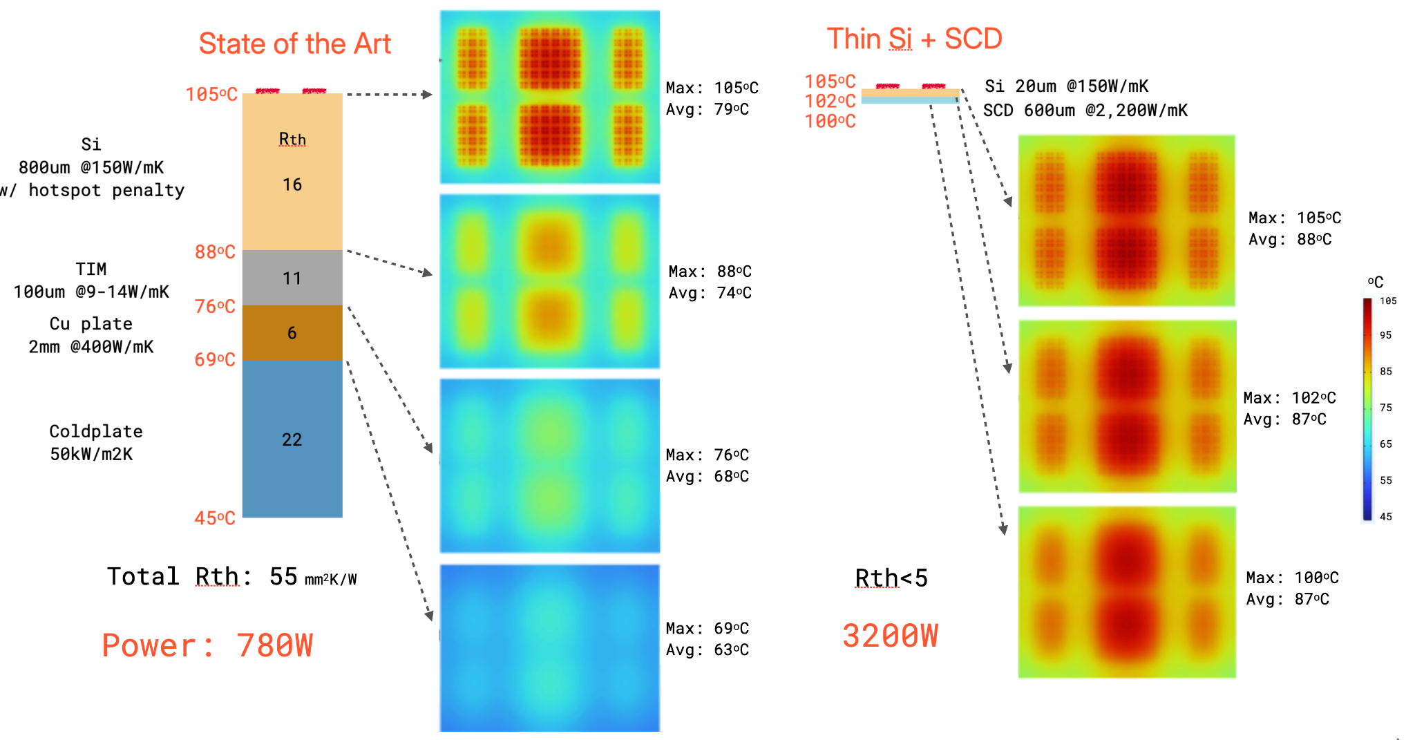
The integration of SCD with thinned silicon reduces upstream thermal resistance and shifts a larger fraction of the temperature drop downstream to be available for higher-performance cooling.
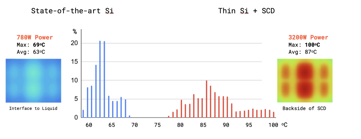
Surface temperature at the cooling interface: 69°C maximum / 63°C average for 780 W silicon; 100°C maximum / 87°C average for 3,200 W thin silicon + SCD.
By making a hotter interface available at the backside of the SCD-substrated chip, advanced two-phase and vapor cooling is enabled very efficiently—including evaporative water cooling at near-atmospheric pressures, featuring maximum capacity.
Reducing resistance inside the package makes more of the available temperature difference useful at the cooling interface.
The effect on required water flow is stark: 10x less than microchannel cooling; and 55× less than a conventional coldplate.
All while delivering 10–100× higher heat removal capability in the cooling system coupled to SCD substrated chips.
Resistance: mm²·K/W
Chip area: 858 mm²
Conventional cold plate
50 kW/m²K
SCD + direct spray
100 kW/m²K
≈80% lower resistance.
Bars share one scale. Numbers inside bars show resistance; +°C labels show each layer’s temperature rise.
*The 4,700 W source case reports a 60°C total rise; its listed layer rises add to 55°C.
These cooling-system comparisons depend on the operating conditions described in the Tech Note.
Microchannels behind a robust SCD substrate can complement its heat spreading. At DF, we favor direct jet impingement on diamond for thermal performance and operational simplicity. Let diamond spread the hotspot heat and keep the fluid system accessible.
Explore the engineering tradeoffs in our cooling article →
Our advanced cooling concept puts liquid directly against the diamond. Thinned silicon is bonded to SCD; an external jet array removes heat from its backside. The thermal path no longer needs a TIM layer or copper cold plate between the diamond and the coolant.
SCD spreads heat from the transistor hotspots and spreads cooling between the jets on its backside. This supports a simpler array of fewer, larger jets with nearby returns. Larger jet diameters can reduce pressure requirements and clogging risk.
Fresh coolant arrives through distributed jets. Nearby return outlets collect warmed fluid locally, limiting the crossflow that would otherwise carry heated liquid across neighboring jets.
Liquid jet cooling can add nucleate boiling, with or without subcooled liquid.
In the subcooled option, the liquid stays below its boiling temperature in the bulk, while the hotter diamond surface supports localized bubble formation. The phase change and fluid mixing increase heat transfer close to the surface.
Jets replenish liquid at the surface, and distributed returns remove spent fluid nearby. Operating pressure, liquid temperature and flow are selected together to sustain surface wetting and effective cooling across the substrate.
A removable manifold is mechanically clamped against a precision O-ring seal at the diamond perimeter. The seal sits outside the active cooling area; the package support carries the clamp load. The SCD substrate has no internal fluid channels, and the external manifold remains accessible for service.
Read more in our Tech Note and learn more about microchannels cooling SCD substrated chips, and why SiC is an incremental thermal advance but not one that achieves AI chip bankability.
Our latest news and industry know-how.

We are working with leaders in cooling technologies on jet impingement, spray and two-phase water cooling.